Low-dimensional heterostructures between semiconducting, superconducting and ferroic materials
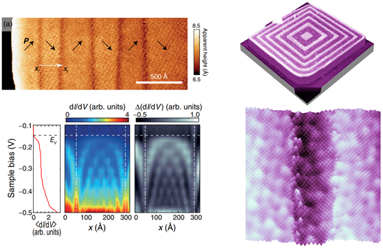
Low-dimensional semiconductors and their heterostructures/superlattices. (Left) STM topography image of a ferroelectric semiconducting SnTe monolayer with sequential 90° domains, and the corresponding dI/dV spectra across one domain revealing electronic standing waves at the valence band maximum, induced by the confinement of domain walls. (Right) Topography images of a SnTe/PbTe semiconducting superlattice. Image size: 200 nm for the upper panel and 20 nm for the lower panel.
Heterostructures between low-dimensional materials are essential for modern electronic devices, including transistors, memory devices, and miniaturized sensors. These heterostructures can be formed using bottom-up methods like molecular beam epitaxy and chemical vapor deposition, or top-down methods like mechanical exfoliation-stacking and ion injection, starting from an atomically flat surface. In solid-state quantum computation, high-performance low-dimensional heterostructures such as Josephson junctions and capacitors in superconducting qubits, 2D electron gas heterostructures in semiconducting quantum dot qubits, and nanowire-superconductor heterostructures in topological qubits are required. Atomic precision is crucial for creating and characterizing these heterostructures to unleash the full potential of quantum materials. Our laboratory focuses on growing both vertical and lateral heterostructures and superlattices between semiconductors, superconductors, ferroelectric, and ferromagnetic materials using molecular beam epitaxy (MBE), which generates atomically sharp interfaces. We observe the interfacial tuning effect through low-temperature scanning tunneling microscopy (STM), which allows us to directly see atoms and surface electronic states in real space. Our interest lies in combining atomically thin/narrow materials to generate novel quantum states of matter, such as topological superconductors, spin-textured semiconductors, and artificial multiferroics, as well as realizing functions such as tunneling memristors and ferroelectric-superconductor transistors. Our studies bridge traditional condensed matter physics and the emerging field of quantum computing.
Address: Building #3, West Area, No.10 Xi-bei-wang East Road, Haidian District, Beijing 100193, P.R. CHINA.